
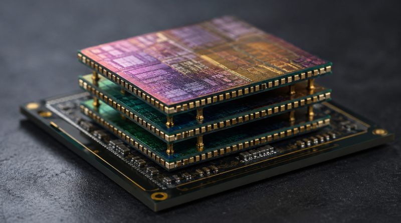
Silicon Goes Vertical: The Three-Layer Chip Built for the AI Age
By stacking ultrathin silicon circuits like floors in a skyscraper, researchers have found a lower temperature route to greater computing power.
The race to build faster computers has traditionally been a race to make everything smaller. For more than half a century, engineers have squeezed increasing numbers of transistors onto flat pieces of silicon, producing processors that are faster, cheaper and more capable with each generation.
Artificial intelligence is now testing the limits of that strategy.
Training and operating advanced AI systems requires immense computing power. Yet the transistors at the heart of modern processors cannot continue shrinking indefinitely. Silicon has physical limits, and at extremely small scales, the strange rules of quantum mechanics begin to interfere with the predictable movement of electrons.
A team of researchers believes the next leap in computing may come not from shrinking chips further, but from building them upward.
In a study published May 27 in Nature, scientists demonstrated a silicon chip containing three vertically stacked layers of transistors. The experimental device was produced using ultrathin silicon membranes and a manufacturing process that required far less heat than conventional chip fabrication.
The approach could offer a practical route to denser, more energy efficient processors, particularly as AI increases demand for both computing capacity and faster data movement.
“Our method is not only easier to implement with lower cost, but it has several advantages over previous approaches to stack silicon wafers,” said Qing Cao, the study’s first author and a professor of materials science and engineering at the University of Illinois Urbana-Champaign.
From a silicon suburb to a skyscraper
Most conventional processors are essentially two-dimensional. Their transistors and electrical connections are arranged across the surface of a silicon wafer. As more components are added, the chip spreads outward, much like a low-rise city expanding into its surrounding land.
That layout creates a growing communication problem. Data must travel between distant parts of a processor and, in many computing systems, between separate chips. Moving information consumes time and energy. In AI applications, where enormous volumes of data are transferred continuously, that movement can become a major bottleneck.
Three-dimensional integration offers another option. By placing active circuits directly above one another, engineers can fit more transistors into the same surface area. The shorter vertical connections also reduce the distance data must travel, potentially increasing speed while lowering the power required for communication.
Cao compared the idea to managing overcrowding in a densely populated city. When there is no room to expand sideways, the solution is to build upward.
The approach could also help extend Moore’s law, the decades-old observation that the number of transistors on a chip tends to double roughly every two years. That steady increase has driven the rapid development of modern electronics, but maintaining it has become increasingly difficult.
Although transistor designs continue to improve, some critical dimensions are no longer shrinking at the rate they once did. One of these is the contacted gate pitch, which includes both the width of a transistor gate and the space separating it from the next transistor.
“If we’re going to keep up the trend of increasing processing power of our microprocessors, we have to start thinking beyond just squeezing more devices on a single surface,” Cao said.
Vertical integration creates additional space without demanding that every component become dramatically smaller.
The heat barrier
The concept of stacking chips is not new. Memory manufacturers already package separate silicon dies on top of one another, and advanced processors increasingly combine specialised components in compact assemblies.
But building multiple high-quality silicon transistor layers directly on the same substrate presents a more difficult challenge.
Manufacturing conventional single-crystalline silicon devices can require temperatures as high as 1,000 degrees Celsius. Those temperatures are manageable when producing the first layer of a chip. Once metal wiring and other delicate structures have been added, however, exposing the device to the same heat can damage or destroy the existing circuitry.
Additional layers therefore have a much smaller thermal budget. They generally need to be fabricated at temperatures below about 400 degrees Celsius.
That restriction has encouraged researchers to use alternative materials for upper transistor layers, including carbon nanotubes, polycrystalline silicon and amorphous or nanocrystalline metal oxides. These materials can be processed at lower temperatures, but they do not always match the performance, consistency and reliability of high-quality single-crystalline silicon.
Cao and his colleagues sought to preserve the advantages of silicon without subjecting the completed lower layers to destructive heat.
Their solution was to manufacture extremely thin silicon nanomembranes separately, then transfer them onto the partially completed chip.
Silicon as thin as a protein
The membranes used by the researchers were no more than 10 nanometres thick. That is roughly comparable to the size of a protein and dramatically thinner than a conventional silicon wafer, which is typically between 500 and 700 micrometres thick.
Because the membranes were so thin, they were also mechanically flexible. Rather than behaving like rigid slabs, they could bend slightly and conform to the microscopic contours of the surface below.
The researchers used a roll laminator to transfer each membrane onto a substrate containing the previous circuit layer. The maximum temperature required to create a strong bond was only 200 degrees Celsius. That is one-fifth of the temperature that may be needed during conventional high-quality silicon processing, and comfortably below the level at which the underlying metal connections could be damaged.
The result was a monolithically integrated chip, meaning its active layers were constructed as part of a single, closely connected device rather than assembled from complete, independently packaged chips.
The prototype contained three silicon layers, with 625 transistors in each layer. Its total of 1,875 transistors is minuscule compared with commercial processors, which can contain tens of billions. But the device was designed to prove that high-quality silicon circuits could be stacked using a process compatible with the delicate structures already in place.
In testing, the chip demonstrated a further advantage. The amount of electrical current flowing through its transistors was at least three to four times greater than in comparable monolithic devices made with alternative upper-layer materials.
That higher current suggests the transistors can deliver stronger performance while retaining the compact geometry and communication benefits of a vertically integrated design.
A promising prototype, not yet a processor
The demonstration does not mean three-dimensional silicon processors are ready to replace today’s chips. Scaling a laboratory device from thousands of transistors to billions will require major advances in manufacturing precision, defect control, wiring, heat removal and production yield.
Operating temperature also remains an important engineering concern. Although the new method reduces the heat required during fabrication, a densely stacked processor would still generate heat while running. Commercial designs would need effective ways to prevent that heat from becoming trapped between active layers.
The researchers nevertheless see the three-layer device as a foundation rather than a limit. In principle, the membrane transfer process could be repeated to add more layers, placing substantially greater computing capacity within the same footprint.
That possibility is especially relevant for AI hardware. Future systems will need not only more transistors, but also architectures that move data quickly and efficiently. Stacking logic and memory closer together could reduce the energy spent transporting information, one of the most persistent problems in modern computing.
For decades, the semiconductor industry advanced by packing more into a flat plane. The new research suggests that the next era may depend on treating silicon less like a sheet of land and more like a skyline.
When there is no longer enough room to spread out, the future of computing may be built one layer at a time.